mSAP - modified semi-additive process
For the realization of even finer conductors (< 25 µm), alternative manufacturing processes have to be applied. One such manufacturing method is conductor build-up using modified semi-additive processes.
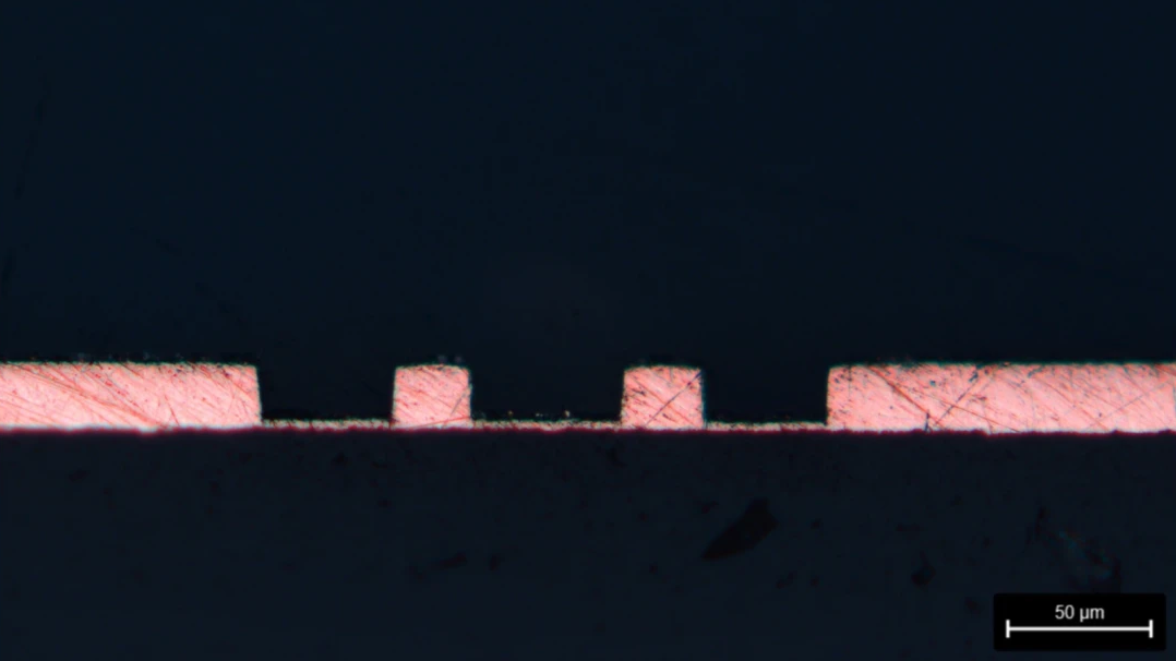
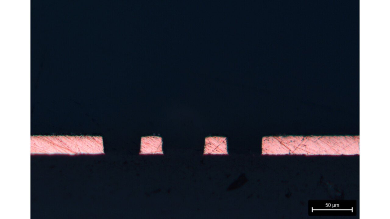
Due to the continuous miniaturization of electronic components, the demands on PCB are increasing. For the realization of even finer conductors (< 25 µm), alternative manufacturing processes have to be applied. One such manufacturing method is conductor build-up using modified semi-additive processes.
In this process, a negative conductor image exposed on a thin conductive layer using photosensitive resists. In the subsequent electroplating process, the desired copper thickness built-up on the exposed areas. After removal of the resist, the built-up conductor pattern retained. The remaining thin layer is removed by flash etching.